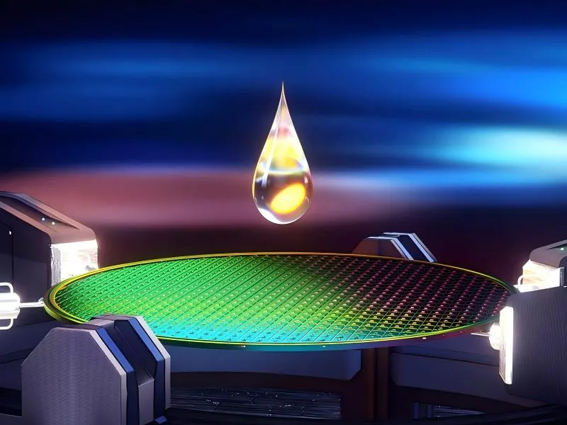
Heynova's photoresist monomers stand out for their exceptional performance. Their unique molecular structure is precisely designed to be highly compatible with various photolithography processes, offering excellent photosensitivity and significantly reducing exposure time. A unique synthesis process ensures high product purity, low impurity levels, and stable, reliable quality. Cost-optimisation strategies make the products extremely cost-effective, helping customers reduce costs and improve efficiency. Heynova leverages innovative technology and stringent quality control to provide core materials for the semiconductor industry, driving technological advancement.
Heynova's photoresist monomer has significant advantages in the semiconductor field:
High purity and low metal impurities: The product purity is extremely high, up to 99.9% or more, the content of key metal ions is as low as 1 ppb or less, to ensure that no impurities will be introduced during the semiconductor manufacturing process to affect the performance of the chip.
High quality standards: The company strictly follows the international quality standards for semiconductor materials and the quality requirements of customers, from raw material procurement to finished product inspection, each link is strictly controlled to ensure that the products excel in resolution, contrast, sensitivity and other key performance indicators to meet the needs of high-end semiconductor manufacturing.
Accurate chemical structure design: In the synthesis process, matching the “customization ability” of the lithography process, we adopt a unique technology to precisely control the molecular structure of the monomer, which is highly adaptable to the semiconductor lithography process.
Technical services and customization capability: Provide full-process services from molecular design, process optimization to mass production support, with the "soft power" to bind high-end customers and molecular design innovation capability.
The process of processing photoresist monomer into resin and photoresist is complex and delicate, and consists of three main stages. Firstly, the monomer is converted into resin through polymerization reaction, and the molecular weight and distribution are precisely controlled; secondly, the resin is formulated into photoresist with photosensitizer (PAC), solvent, etc., and filtered to ensure the cleanliness; and the final product is widely used in semiconductor manufacturing (DUV/EUV lithography), display panels (OLED/LCD), and advanced packaging (TSV/RDL). Through precise control of the polymerization process and formulation optimization, the photoresist pattern residual rate in semiconductor etching meets the requirements of advanced processes. With technological advances, the new generation of photoresists is moving toward higher resolution, higher sensitivity and better etch selection ratio, while environmentally friendly formulations are increasingly emphasized.
