Applications of PSPI in Semiconductors and OLEDs
In the semiconductor industry, PSPI can be used for wafer passivation and stress relief layers. Negative-develop PSPI can form films ranging from several micrometers to tens of micrometers thick in a single coating, providing both passivation protection and stress relief. It mitigates warpage and cracking caused by thermal expansion mismatches between the chip and the packaging substrate, serving as the core dielectric layer in fan-out packaging. PSPI can also be used in redistribution layers (RDLs). Positive-type PSPI is used in photolithography to fabricate micrometer-scale vias, enabling the re-routing of chip I/O. This application requires high resolution, low dielectric constant, and low metal ion content, making PSPI a key insulating material for 2.5D/3D packaging. PSPI can also be used in interlayer insulation and TSV insulation layers to suppress copper diffusion and isolate the silicon substrate, supporting high-density heterogeneous integration. In semiconductor applications, low CTE, low residual stress, and extremely low metal ion purity are particularly critical.
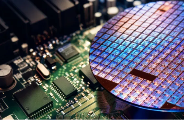
In the field of OLED displays, PSPI is primarily based on a negative system, with a single material serving multiple functions:
Pixel Definition Layer (PDL): Photolithographically forms pixel apertures and isolates adjacent subpixels; the angle of its sidewalls must be precisely controlled between 20oand 30o, which directly determines the vapor deposition yield and display resolution;
Planarization Layer (PLN): Fills in the steps of the TFT backplane metal lines to ensure uniform film deposition of the emissive layer;
Spacer Columns: Support precision metal masks to prevent scratching of the emissive layer. PSPI for OLEDs must feature high visible light transmittance, low outgassing, resistance to high-temperature vapor deposition, and low-temperature curing (230~270oC) to avoid damaging TFT devices.
Oligomeric PSPI
Traditional PSPI matrices are based on high-molecular-weight polyacrylamide (PAA), with a number-average molecular weight (Mn) in the tens of thousands. High-molecular-weight PAA has inherent drawbacks: high viscosity, making it difficult to apply thick films at high solid content; severe molecular chain entanglement; high internal stress caused by solvent evaporation and ring-closing dehydration during thermal imidization, leading to film warping and cracking; difficulty of developing solvents in penetrating thick films, resulting in poor quality of pattern sidewalls; and restricted chain segment mobility, leading to low reaction efficiency of photosensitive groups. These issues are particularly pronounced on large-size wafers, thin wafers, and flexible substrates. Conventional PAA is a long-chain polymer, whereas the oligomer PSPI is a short-chain oligomer with a controlled low degree of polymerization (Mn approximately 1000~8000)—it can be either an oligomeric PAA or a pre-imide-ized PI oligomer—and photosensitive functional groups can be introduced at the terminal groups or side chains, representing an independent material design concept.
Oligomeric PSPI offers significant advantages over conventional PSPI:
Improved processability: Solution viscosity is significantly reduced at the same solid content, enabling high-solid-content, low-viscosity formulations, single-pass thick-film coating, and a reduction in the number of layers;Substantially reduced residual stress: Weakened short-chain entanglement leads to reduced imidization shrinkage and stress, significantly lowering the risk of wafer warpage and film cracking—which is particularly important for low-stress dielectric layers;Improved photolithography performance: Development solvents penetrate more easily, ensuring uniform development; photosensitive groups have lower steric hindrance, enhancing reaction efficiency and resolution;Enables low-temperature curing: Enhanced mobility of short-chain molecules lowers the ring-closing imidization temperature, making it suitable for high-temperature-sensitive substrates such as flexible OLED backplanes;Impurities are easier to control: A narrow molecular weight distribution can be regulated through purification, helping to reduce metal ions and particulates. The trade-off is that an excessively low molecular weight sacrifices the mechanical strength and elongation at break of the PI after curing, which must be compensated for through a design featuring cross-linkable terminal groups.
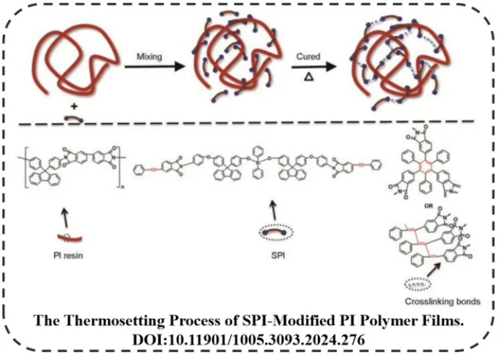
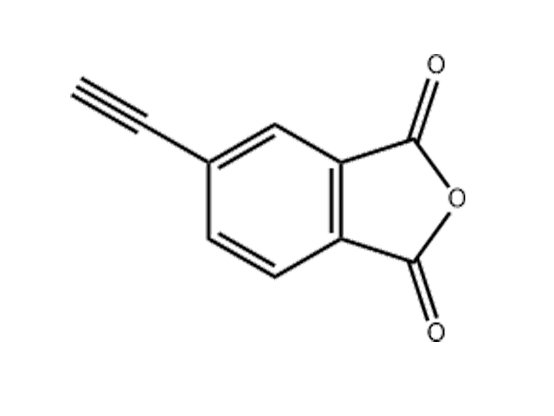
Currently, there are two mainstream synthetic routes for PSPI oligomers. The first involves synthesizing end-functionalized polyamido acid by controlling the molar ratio of dianhydride to diamine, followed by blending with photosensitive components; The second involves using a monofunctional capping agent to limit the degree of polymerization and directly introducing photo-crosslinkable end groups (such as vinyl, acrylate, or maleimide) to achieve a balance between “low viscosity, low stress, and crosslinkable mechanical compensation.” The overall trend in PSPI oligomers is toward lower residual stress, low-temperature curing, higher resolution, and lower ionic impurities to meet the process requirements of large-size wafers and flexible OLEDs. With its outstanding advantages of low viscosity, low residual stress, and low-temperature curing—which effectively overcome the inherent shortcomings of traditional PAA polymer systems—oligomer PSPI represents an important research direction for next-generation dielectric materials. However, molecular structure design must balance the loss of mechanical and thermal stability resulting from low molecular weight, and end-capping and crosslinking design, impurity control, and molecular weight distribution regulation remain the core focus of future R&D.
HEYNOVA
an excellent service provider of key new materials and overall solutions for the global high-tech industry, focusing on the R&D and production of Polyimide monomer, Photoresist monomer & PAG, OLED monomer, Lithium battery materials, and customized services.


 English
 Nederland


-new-material-technology-co.,-ltd.-wechat.webp)