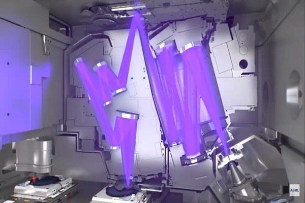
The core mechanism of EUV photoresist involves a chain reaction triggered by high-energy photons: ionization→electron conduction→chemical transformation→solubility differentiation. Its essence lies in converting the energy of 13.5 nm extreme ultraviolet light into chemical property differences within microscopic regions of the photoresist, thereby achieving precise circuit pattern transfer. Unlike traditional deep ultraviolet (DUV) photoresists, which rely on ultraviolet light to induce simple intermolecular cross-linking or cleavage, the reaction process of EUV photoresists involves the interdisciplinary integration of high-energy plasma physics, radiochemistry, and polymer science. Additionally, it must be adapted to the vacuum environment and total internal reflection optical systems characteristic of EUV lithography.

The defining characteristic of EUV lithography is the exceptionally high energy of its 13.5 nm photons (approximately 92.3 eV). This energy far exceeds that of traditional DUV lithography (ArF lithography photons have an energy of only 19.7 eV) and is significantly higher than the bond energies within photoresist molecules. Consequently, the first step in EUV photoresist processing is not the direct triggering of chemical bond breaking, but rather photoionization. In an ultra-high vacuum environment, when EUV photons strike the photoresist film, their energy is absorbed by electrons within the molecules. This causes electrons to transition from their ground state to an ionized state, forming photoelectrons, while the molecules themselves become cationic radicals.
Primary photoelectrons possess energies reaching tens of electronvolts, far exceeding the energy required for chemical bond breaking. Rather than directly participating in chemical reactions, they collide with surrounding photoresist molecules, triggering secondary electron emission—the core intermediate step in EUV photoresist reactions. A single primary photoelectron can excite 10~20 secondary electrons, achieving energy “multiplication”. The efficiency of this process directly determines the photoresist's sensitivity. Low secondary electron yield results in significant energy loss from primary electrons, requiring higher exposure doses to trigger subsequent reactions.
The energy carried by secondary electrons precisely triggers chemical reactions within the photoresist's functional groups. Activation mechanisms vary significantly among different types of EUV photoresists.
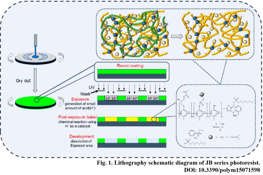
Chemically amplified photoresists (CAP) represent the mainstream commercial EUV photoresist type, with PAG serving as their core functional group. When secondary electrons collide with PAG molecules, they break internal ionic or covalent bonds, causing PAG decomposition and releasing strong acids (e.g., perfluorosulfonic acid). These strong acids act as catalysts during the subsequent post-exposure baking (PEB) process, catalyzing the deprotection reaction of acid-sensitive groups within the photoresist matrix. Compared to traditional DUV chemically amplified resists, PAG requires covalent bonding with the polymer matrix to prevent migration or volatilization in vacuum environments while reducing LER issues caused by uneven PAG dispersion.

Metal oxide photoresists primarily consist of oxides or oxides of metals such as tungsten, hafnium, and tin. Their activation mechanism relies on the direct interaction of secondary electrons with metal-oxygen (M-O) bonds. The high-energy impact of secondary electrons breaks the M-O bonds, causing metal ions to dissociate from the stable oxide lattice and form low-oxidation-state metal atoms or ions. Metal ions in the exposed regions undergo complexation reactions in the developer solution, forming soluble metal complexes that are washed away. In contrast, the M-O lattice in unexposed areas remains intact and insoluble in the developer, ultimately forming a negative photolithographic pattern.
Molecular glass photoresists utilize functionalized small molecules as their matrix. Their activation process lacks intermediate catalytic steps, classifying them as “direct-reaction type”. Secondary electrons directly act upon sensitive bonds (e.g., ester bonds, azide bonds) within the small molecules, causing cleavage or cross-linking in the exposed regions. Due to the uniform molecular weight distribution of these small molecules, the sites of secondary electron interaction are more controllable, enabling LER reduction below 1.5 nm. This makes them a core candidate for future advanced process technologies.
For chemically amplified photoresists, post-bake accelerates strong acid diffusion, enabling more complete deprotection of acid-sensitive groups while eliminating local reaction inhomogeneities. For metal oxide photoresists, post-bake solidifies the M-O lattice in unexposed regions, enhancing etch resistance. Post-bake temperature control demands extreme precision. Excessive heat causes acid overdiffusion, inducing pattern distortion; insufficient heat results in incomplete reactions, reducing development contrast.
Positive chemically amplified photoresists typically employ tetramethylammonium hydroxide (TMAH) alkaline developers. Carboxyl groups in exposed areas react with TMAH to form soluble carboxylates, which are then eluted by the developer. In contrast, metal oxide photoresists commonly use acidic complexing developers (e.g., ammonium citrate solutions) that dissolve metal ions in exposed regions through complexation. The critical aspects of the development process are controlling the development rate and time. Underdevelopment leads to pattern residue, while overdevelopment causes line width shrinkage. Precise control based on the reactivity of the photoresist is essential.
After development, the photoresist circuit patterns undergo a resist hardening bake (150~200oC) to solidify and enhance tolerance for subsequent processes like etching and ion implantation. This stage demands stringent thermal stability from the photoresist. If photoresist decomposition or deformation occurs during bake, circuit patterns will fail. Consequently, metal oxide photoresists, capable of withstanding temperatures above 300oC, hold a distinct advantage in high-end manufacturing processes.

Contact us to learn more about our advanced electronic chemicals and speciality polymer materials, and how they can enhance your production performances.