In the fields of semiconductor and micro-nano manufacturing, lithography technology is the cornerstone that defines the precision structures of chips and optical devices. While EUV and DUV lithography—well-known to the general public—are primarily used for large-scale mass production, electron beam lithography (EBL) represents the “ultimate limit of precision” in scientific research and high-end mold manufacturing. Requiring no optical masks and unconstrained by the diffraction limit, it is currently the micro- and nano-pattern formation technology with the highest controllable precision available to humanity, and serves as the core fabrication process for nanoimprint masters, high-end optical masks, and cutting-edge quantum devices.
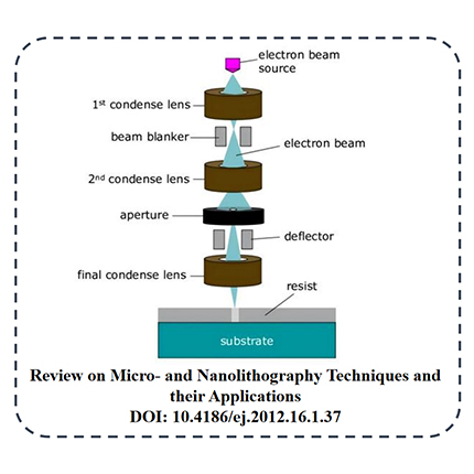
From a fundamental principles perspective, electron beam lithography differs fundamentally from traditional optical lithography. Optical lithography relies on projecting images using light of a specific wavelength and is limited by diffraction effects, resulting in an inherent upper limit on resolution; EBL, on the other hand, utilizes a high-energy focused electron beam as a “nano-pen,” leveraging the extremely short physical wavelength of electrons (on the order of just 0.01 nm) to completely overcome the constraints of the diffraction limit. Operating in a high-vacuum environment, the equipment uses electromagnetic lenses to focus the electron beam into an ultra-fine spot measuring just a few nanometers. A computer reads the pattern data and controls the electron beam to scan, point by point, across a substrate coated with electron-sensitive resist. By altering the solubility of the resist with the electron beam, high-precision nanoscale patterns are obtained after development. The entire process requires no physical masks, allowing for flexible and efficient design iterations.
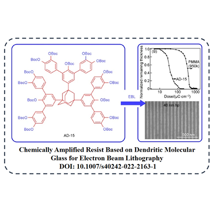
The selection of suitable photoresist materials is key to achieving precise patterning in EBL. There are three main categories, each with a distinct role and suited to different process scenarios. First is PMMA (polymethyl methacrylate), a general-purpose positive resist that is low-cost, simple to process, and easy to strip completely. Conventional processes can stably achieve line widths of 10~15 nm, and with optimized low-temperature processes, this can be reduced to 5~8 nm. It is the material of choice for conventional quartz master templates in nanoimprinting and is widely used in the fabrication of standard nanograting and microporous structures. Second is HSQ (hydrogen silsesquioxane), an inorganic negative resist and a core material for high-precision processes. It offers resolutions of 3~8 nm and exhibits extremely high resistance to dry etching; once cross-linked, the structure is hard and stable. It is specifically used for ultra-fine nanostructures, high aspect ratio hard masks, and EUV mask patterning. Finally, there is SU-8 epoxy resist, which is primarily used for ultra-thick film processing and can form resist layers hundreds of micrometers thick. It is suitable for micrometer-scale structures with high aspect ratios, but its resolution is only at the micrometer level, making it unsuitable for nanoscale precision processing. It is primarily used in the fabrication of MEMS devices, microfluidic chips, and electroforming molds.
Thanks to its unique technical characteristics, EBL offers irreplaceable core advantages. First, it delivers unparalleled resolution, with a laboratory limit of less than 3 nm, making it the mainstream process currently capable of reliably fabricating precision patterns smaller than 10 nm. Second, its mask-less direct writing offers high flexibility; it eliminates the need for expensive custom masks, allows for easy layout modifications, and is well-suited for iterative research and small-batch customization; Third, it offers exceptional substrate compatibility, capable of processing various materials such as silicon, quartz, glass, and compound semiconductors, covering the vast majority of micro- and nano-device R&D scenarios; finally, it delivers low edge roughness and excellent imaging quality, meeting the high-precision requirements of metamaterials, quantum devices, and other applications.
However, EBL’s inherent limitations mean it cannot replace EUV or DUV for large-scale wafer mass production. The most critical issue is its extremely low throughput; the point-by-point scanning mode means that exposing a single substrate takes hours or even days, making it completely unsuitable for the mass production of large wafers. Secondly, there are defects caused by the proximity effect: electron scattering leads to uneven exposure of dense lines, requiring complex algorithms for correction. At the same time, insulating substrates are prone to charge accumulation, causing pattern shift and distortion, resulting in a low process tolerance. Furthermore, the equipment is expensive to build and requires a high level of expertise for operation and maintenance; the cost per wafer for small-batch processing is extremely high, making it severely uneconomical for mass production. In industrial applications, EBL has precisely positioned itself in high-end niche markets, forming a complementary ecosystem with EUV and nanoimprint lithography. While it is not used for the mass production of consumer-grade chips, it serves as a core upstream process for the fabrication of high-end master templates; all high-precision nanoimprint hard templates and EUV optical masks must be fabricated using EBL.
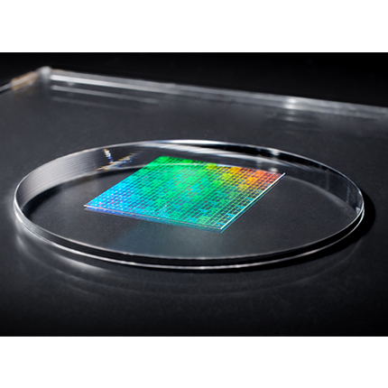
In summary, electron beam lithography is not a “production line” for mass production, but rather a “precision engraving machine” in the field of nanomanufacturing. With its unparalleled precision, it fills a technological gap in high-end micro- and nano-processing, bridging the gap between scientific research and innovation and industrial application. It serves as a core upstream support for nanoimprinting and advanced lithography technologies, and is also one of the key technologies driving breakthroughs in China’s micro- and nano-manufacturing and the localization of high-end semiconductor equipment.
HEYNOVA
an excellent service provider of key new materials and overall solutions for the global high-tech industry, focusing on the R&D and production of Polyimide monomer, Photoresist monomer & PAG, OLED monomer, Lithium battery materials, and customized services.


 English
 Nederland




-new-material-technology-co.,-ltd.-wechat.webp)