As chip manufacturing processes advance toward the 2 nm and 1 nm nodes, traditional chemical amplification resist (CAR) is gradually reaching its performance limits. Issues such as low EUV photon absorption efficiency, pattern roughness caused by acid diffusion, and insufficient etch resistance severely limit the precision of ultra-high-resolution pattern fabrication. Against this backdrop, metal oxide photoresists (MORs), with their inorganic-organic hybrid structure, ultra-high EUV sensitivity, and excellent etch resistance, have emerged as the leading candidate photoresist materials for the high-NA EUV era and represent a current research hotspot in the field of semiconductor lithography.
Metal oxide photoresists are a class of negative-type photoresists centered on metal-oxygen clusters. Their core structure differs from that of traditional polymer photoresists, consisting of an inorganic metal-oxygen core, organic carboxylic acid ligands, organic solvents, and trace additives. Mainstream systems fall into two categories: first, Group IVB zirconium (Zr) and hafnium (Hf) metal-oxygen clusters, which offer high stability and top-tier etch resistance; second, tin (Sn) metal-oxygen clusters, which feature an extremely high EUV photon absorption cross-section and excellent photosensitivity, making them a key focus for industrialization. Their microstructure consists of a nanoscale core-shell architecture, in which the inorganic metal-oxygen core forms a rigid framework, and organic carboxylic acid ligands are bound to the surface via M-O coordination bonds—this serves as the core structural foundation for stable imaging.
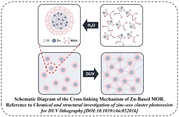
Its unique structure endows it with an entirely new imaging mechanism, completely breaking away from the acid-diffusion imaging mode of traditional CAR photoresists. When the photoresist is unexposed, intact organic ligands surround the metal-oxygen clusters, rendering the material soluble in organic solvents; after exposure to EUV or an electron beam, the metal nuclei efficiently absorb photons to generate a large number of secondary electrons, which drive the breaking of surface M-O coordination bonds and trigger a decarboxylation reaction to remove the organic ligands. The exposed metal active sites bond with one another to form a dense M-O-M inorganic cross-linked network that is no longer soluble in organic solvents. Finally, through development with an organic solvent, the soluble oxygen clusters in the unexposed areas are washed away, while the exposed, cross-linked areas are retained, thereby completing the formation of a negative-type nanopattern.
Compared to traditional organic photoresists, metal oxide photoresists offer significant technical advantages. First, they exhibit no swelling and high precision. When traditional organic negative photoresists are developed using organic solvents, the flexible polymer network is easily penetrated and swollen by the solvent, leading to line width shifts and rough edges. In contrast, MOR forms a rigid inorganic framework after exposure, with minimal free volume, resulting in virtually no swelling issues. This significantly reduces line edge roughness (LER) and is suitable for single-digit nanometer processes. Second, it offers a higher performance ceiling. The high EUV absorption efficiency of metal atoms, combined with excellent high-temperature resistance and resistance to plasma etching, solves the challenge of pattern transfer in ultra-thin photoresist films, making it perfectly suited for high-NA EUV shallow depth-of-field processes.
Of course, this material still has some shortcomings that are difficult to avoid at this stage. Unlike traditional photoresists, which are compatible with 2.38% TMAH aqueous developer solutions, metal oxide photoresists must be developed using organic solvents such as IPA and ethyl acetate. This continues to pose environmental pollution issues related to VOCs, and the waste liquid contains heavy metal components, resulting in higher treatment costs. At the same time, the material suffers from stability issues. The overall stability ranking is Hf oxocluster > Zr oxocluster > Sn oxocluster. Sn oxoclusters are highly sensitive to moisture and temperature; their solutions have a short storage life, and the films are prone to aging. The post-exposure delay (PED) effect can easily cause pattern defects, making mass production processes far more challenging than those for traditional photoresists.
Currently, metal oxide photoresists have established a clear matrix of application scenarios. The semiconductor sector is the core market, with widespread use in EUV lithography processes for logic chips, DRAM, and NAND memory chips at 7 nm and below; they are also compatible with electron beam lithography for the fabrication of high-precision lithographic masks. In the field of micro- and nano-manufacturing, they can be used to fabricate MEMS devices and microfluidic structures with high aspect ratios, and their high-temperature resistance prevents pattern deformation in subsequent processes. Furthermore, they can be applied in cutting-edge fields such as the fabrication of micro- and nano-scale photonic structures and ceramic micro- and nano-scale 3D printing, making them a new type of photoresist material that balances ultra-high resolution with functional adaptability.

HEYNOVA
an excellent service provider of key new materials and overall solutions for the global high-tech industry, focusing on the R&D and production of Polyimide monomer, Photoresist monomer & PAG, OLED monomer, Lithium battery materials, and customized services.


 English
 Nederland



-new-material-technology-co.,-ltd.-wechat.webp)