For a long time, improvements in integrated circuit performance have relied primarily on Moore’s Law, which states that the number of transistors that can be accommodated on an integrated circuit doubles every 18 to 24 months. This progress would not have been possible without the relentless efforts of lithography technology in scaling down feature sizes. From mercury-vapor lamps to deep ultraviolet (DUV) and extreme ultraviolet (EUV) lithography, each upgrade in light sources has been accompanied by massive technological investments and increased process complexity. However, as feature sizes have entered the nanometer range, issues such as diffraction effects, exposure uniformity, and mask fabrication have become increasingly prominent, causing the cost of traditional lithography to rise exponentially and putting its economic viability and technical feasibility to a severe test.
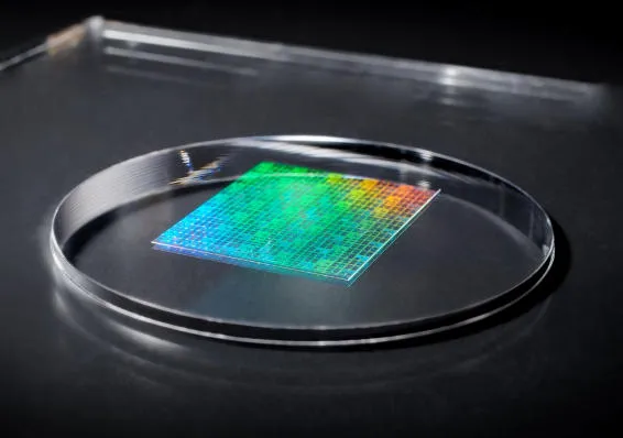
It was against this backdrop that nanoimprint technology emerged. Unlike the complex “exposure-development-etching” process of traditional lithography, the core concept of nanoimprint technology is more akin to “stamping”—that is, using mechanical imprinting to transfer nanoscale patterns directly from a finely patterned mold to the photoresist materials (resist) on the substrate. This direct pattern transfer method, in principle, overcomes the limitations of the diffraction limit, enabling the fabrication of ultra-high-resolution nanopatterns at a relatively low cost.
Nanoimprint technology can be broadly categorized into several types, including hot embossing, UV nanoimprint lithography, and soft nanoimprint lithography.
·Hot Embossing: This was the first nanoimprint technology to be proposed. It works by heating a polymer film on the substrate to a temperature above its glass transition temperature, causing it to soften. Then, a nano-patterned mold is pressed into the softened polymer using high pressure. After cooling, the polymer solidifies, and the pattern is replicated onto the polymer film. Finally, the pattern is transferred to the substrate material through subsequent processes such as etching. The advantage of thermal nanoimprinting is that the process is relatively simple and suitable for a wide range of polymer materials. However, a disadvantage is that the high imprinting temperature can lead to mismatched thermal expansion between the mold and the substrate, thereby affecting pattern accuracy and yield.
·UV Nanoimprinting: To overcome the drawbacks of thermal nanoimprinting, UV nanoimprinting technology was developed. It uses UV-curable resin as the imprinting material. At room temperature, a low-viscosity UV-curable resin is drop-coated onto the substrate, and then a transparent mold is pressed into the resin. Upon exposure to UV light, the resin rapidly cures, forming a solid film bearing the mold’s pattern. The advantages of UV nanoimprinting include low imprinting temperatures, fast imprinting speeds, high pattern accuracy, and better compatibility with semiconductor processes; it is currently one of the most widely researched and applied nanoimprinting technologies.

·Soft Nanimprinting: Soft nanimprinting technology uses elastomers (such as PDMS) as the mold material. Because elastic molds are flexible, they can better conform to uneven substrate surfaces, thereby reducing defects. This technology is particularly suitable for fabricating nanostructures on flexible substrates or for large-area patterning.
The resolution of nanoimprint technology primarily depends on the precision of the mold fabrication; theoretically, it can reach the nanometer or even sub-nanometer scale, breaking through the diffraction limit of traditional lithography and offering tremendous potential in the field of high-density, highly integrated device manufacturing. Compared to EUV lithography, which involves equipment costs of hundreds of millions of dollars as well as specialized euv photoresist, nanoimprinting requires a lower investment and eliminates the need for expensive mask fabrication and complex optical systems, resulting in more competitive production costs. UV nanoimprinting features fast curing speeds, and roll-to-roll processes enable large-scale, low-cost production of flexible electronics. Additionally, it can achieve complex three-dimensional nanostructures through multi-layer imprinting or specialized molds, offering unique advantages in fields such as micro- and nano-optics and biomedical devices. However, its industrialization still faces challenges: precision control of nano-molds; lifespan and cost issues caused by wear and contamination; precise regulation of the imprint residue layer; defects and yield bottlenecks resulting from particles, bubbles, and alignment errors; and the need for research and development of high-performance imprinting materials. With continuous breakthroughs in mold technology, equipment processes, and new materials, nanoimprint technology is gradually moving from the laboratory toward industrial applications in fields such as storage devices, logic chips, LEDs, and biosensors.
HEYNOVA
an excellent service provider of key new materials and overall solutions for the global high-tech industry, focusing on the R&D and production of Polyimide monomer, Photoresist monomer & PAG, OLED monomer, Lithium battery materials, and customized services.


 English
 Nederland


![Ethanone,1,1'-[1,3-Propanediylbis(Oxy-4,1-Phenylene)]bis[2,2,2-Trifluoro-,1,1'-Bis[o-(Propylsulfonyl)oxime] 300374-81-6 C25H28F6N2O8S2](/uploads/image/20250709/300374-81-6-china.webp "Ethanone,1,1'-[1,3-Propanediylbis(Oxy-4,1-Phenylene)]bis[2,2,2-Trifluoro-,1,1'-Bis[o-(Propylsulfonyl)oxime] 300374-81-6 C25H28F6N2O8S2")
![2-[3'-(9,9-Dimethyl-9H-fluoren-2-yl)[1,1'-biphenyl]-3-yl]-4,6-diphenyl-1,3,5-triazine 1955543-57-3 C42H31N3](/uploads/image/20251017/1955543-57-3-china.webp "2-[3'-(9,9-Dimethyl-9H-fluoren-2-yl)[1,1'-biphenyl]-3-yl]-4,6-diphenyl-1,3,5-triazine 1955543-57-3 C42H31N3")
-new-material-technology-co.,-ltd.-wechat.webp)