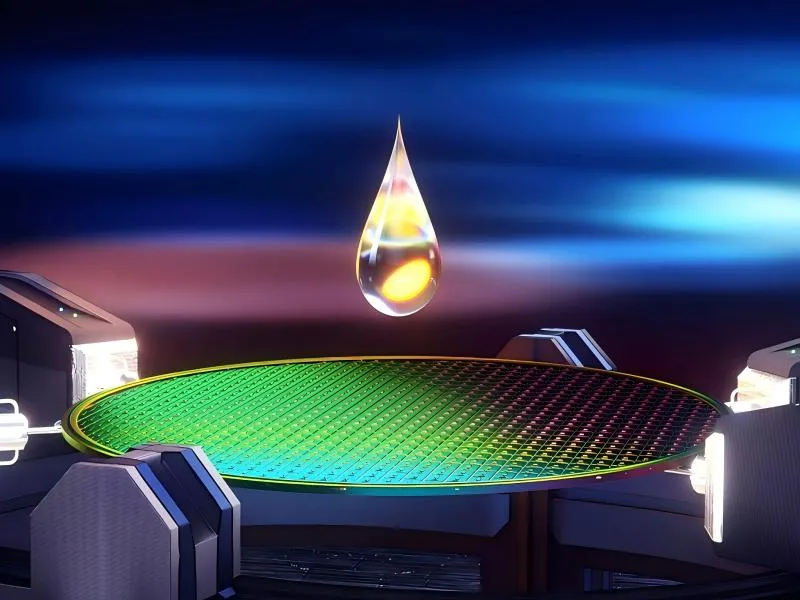
The company's PAC, with its excellent performance and wide range of applications, has become an important choice in the photoresist field. Its absorption of specific wavelengths of light is extremely efficient, can quickly trigger photochemical reactions, generating a large number of active intermediates, sensitivity far more than similar products, significantly shorten the exposure time, improve production efficiency. And good compatibility with phenolic resin and other commonly used photoresist materials, can be uniformly dispersed, the synergistic effect is stable, to ensure that the photoresist performance to give full play to.
The company's photosensitizer PAC products have three core advantages:
High reactivity: Adopting optimized molecular structure design, the photolysis efficiency is increased by 40%, which significantly reduces the exposure dose requirement and lowers the production cost;
Excellent resolution: Sub-micron graphic transfer in the 248nm/365nm band, line width roughness (LER) <1.5nm, to meet the needs of 14nm and above process;
Excellent process stability: Perfect compatibility with phenolic resin and other base materials, good thermal stability, stable performance between batches.
The company's PAC products have realized breakthroughs in the above dimensions through molecular structure innovations (e.g., thick cyclic aromatic hydrocarbon derivatives), and have already supported the mass production of a number of domestic foundries.
The company's photosensitizer (PAC) products play a key role in the semiconductor lithography process. In the field of display panels, PAC products help positive photoresists to image accurately, so that the circuit patterns of TFT-LCD and OLED panels are clear and the lines are fine, which effectively improves the display resolution and color saturation, and brings better visual experience for users.
In semiconductor chip manufacturing, for i-line and g-line photoresists, PAC absorbs specific wavelengths of light and rapidly triggers photochemical reactions to accurately control the dissolution or cross-linking of the photoresist, realizing high-resolution transfer of the chip circuit pattern and guaranteeing chip performance and integration.
In addition, in the semiconductor packaging process, PAC is used as the key raw material of positive adhesive to ensure the precise molding of structural patterns such as pins and pads during the encapsulation photolithography process, thus enhancing the reliability of encapsulation.
