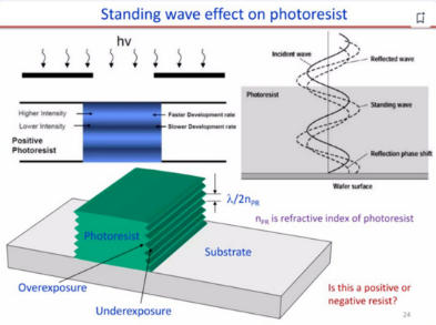
Against the backdrop of continuous scaling in advanced semiconductor processes, 193 nm immersion lithography has long supported the mass production of 28 nm to 7 nm logic chips, 3D NAND memory, and DRAM with multiple patterning, thanks to its exceptional process stability and cost advantages. However, with the increase in numerical aperture (NA), the continuous reduction in thickness of photoresist materials, the growing complexity of wafer surface topography, and the widespread use of highly reflective metal materials, the traditional process architecture—which combines a single-layer photoresist with an organic BARC—has gradually revealed numerous shortcomings. These include severe standing wave effects, critical dimension fluctuations, pattern notching, degradation of line edge roughness, and distortion of etched patterns with high aspect ratios. To address these bottlenecks, the industry has widely adopted a three-layer spin-coating architecture consisting of photoresist, Si-BARC, and SOC. By leveraging the strong-absorbing SOC underlayer and the Si-BARC silicon-based interference layer to form a dual-layer anti-reflection system, this approach achieves a three-in-one process capability that combines optical noise reduction, surface planarization, and high selectivity hard mask transfer.
Development and Architectural Evolution of Multi-Layer Anti-Reflection Coating (BARC) Technology
Early KrF and conventional ArF lithography generally employed a two-layer structure consisting of “photoresist + a single layer of organic BARC,” relying on the UV absorption capacity of organic resins to reduce substrate reflection. However, this system has an inherent flaw: the thickness of a single-layer BARC is limited, making it unable to fill the steps and grooves on the wafer, which leads to uneven photoresist thickness and significant “swing” line width fluctuations. At the same time, the extinction capacity of organic BARC is limited; on highly reflective metal substrates, residual reflected light remains strong, resulting in pronounced standing wave fringes and high pattern sidewall roughness. Most critically, conventional organic BARC does not contain silicon; its oxygen plasma etch rate is similar to that of photoresist, making it incapable of forming an effective hard mask and rendering it unsuitable for the high aspect ratio pattern transfer required by advanced processes.
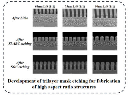
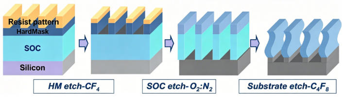
To address this, advanced 193 nm immersion lithography introduces a three-layer architecture with distinct functional roles: the top-layer photoresist is responsible solely for photolithographic imaging; the middle Si-BARC layer handles optical interference-based anti-reflection and serves as a transition to the silicon-based hard mask; and the bottom-layer SOC achieves global planarization and absorbs the primary UV radiation. Together, the SOC and Si-BARC form a dual-layer anti-reflection system that suppresses substrate reflectance to below 1%. At the same time, they enable stepwise pattern transfer through a high etch selectivity ratio, thereby completely resolving the performance limitations of traditional single-layer anti-reflection solutions.
Material Properties and Core Functions of SOC Spin-On Carbon Coatings
SOC (Spin-On Carbon) serves as the bottom support layer and primary anti-absorption layer in a three-layer photolithography system. It is a high-carbon-content aromatic thermosetting resin system with a carbon mass fraction ranging from 80% to 92% and virtually no silicon. Its molecular framework consists primarily of fused-ring aromatics and phenolic conjugated structures, and exhibits excellent 193 nm UV absorption properties and high-temperature thermal stability. After cross-linking and curing at high temperatures of 250~320oC, SOC forms a dense, insoluble, and infusible amorphous-like carbon film, serving as the functional cornerstone of the entire three-layer architecture.
SOC possesses three irreplaceable core capabilities. First is global topographic flattening. SOC films can reach thicknesses of 200~500 nm, far exceeding those of traditional BARC films. The spin-coating process relies on the fluid’s self-leveling properties to fully fill wafer grooves, metal steps, and dense pattern variations, ensuring uniform film thickness for the overlying Si-BARC and photoresist layers. This eliminates CD drift and the swing effect caused by photoresist thickness fluctuations at the source. Second is its exceptional light-absorbing properties at the substrate level. SOC has an extinction coefficient k > 1.0 in the 193 nm wavelength band, significantly higher than that of organic BARC and Si-BARC. It absorbs the vast majority of exposure photons that penetrate the upper layers, greatly reducing the energy of reflected light from the substrate and achieving first-order optical attenuation. Third is its function as a thick-film hard mask with a high selectivity ratio. The pure carbon structure exhibits an extremely fast etch rate during oxygen plasma etching, achieving an etch selectivity ratio of over 10:1 compared to silicon-containing Si-BARC. It can serve as the primary mask to complete deep etching of the substrate, protecting the fine patterns in the upper layers from damage.
The main resins used in mass-produced SOCs are typically copolymers of highly conjugated monomers such as naphthol, biphenyl-1,2-diol, and BHPF (fluorenylphenol). Depending on process requirements, they can be classified into three categories: conventional planar types, high-fill trench types, and low-hydrogen resist types, which are respectively suited for standard logic layers, deep structures in 3D NAND, and multi-patterning processes below 7 nm.

HEYNOVA
an excellent service provider of key new materials and overall solutions for the global high-tech industry, focusing on the R&D and production of Polyimide monomer, Photoresist monomer & PAG, OLED monomer, Lithium battery materials, and customized services.


 English
 Nederland


![2-{3'-Bromo-[1,1'-Biphenyl]-3-Yl}-4,6-Diphenyl-1,3,5-Triazine 1606981-69-4 C27H18BrN3](/uploads/image/20250714/1606981-69-4-china.webp "2-{3'-Bromo-[1,1'-Biphenyl]-3-Yl}-4,6-Diphenyl-1,3,5-Triazine 1606981-69-4 C27H18BrN3")
![3,6-Di(9H-carbazol-9-yl)benzo[4,5]thieno[2,3-b]pyridine 1235883-57-4 C35H21N3S](/uploads/image/20251017/1235883-57-4-china.webp "3,6-Di(9H-carbazol-9-yl)benzo[4,5]thieno[2,3-b]pyridine 1235883-57-4 C35H21N3S")
-new-material-technology-co.,-ltd.-wechat.webp)