Optical Proximity Effect (OPE) in lithography refers to the deviation between the actual pattern formed on photoresist and the designed pattern on the mask plate, caused by optical phenomena such as diffraction and interference during the lithography process. It is one of the core issues affecting pattern fidelity in nanoscale lithography, directly impacting the dimensional accuracy and performance reliability of semiconductor devices.

Lithography fundamentally involves projecting mask patterns onto photoresist through optical systems. When feature sizes approach or fall below half the exposure wavelength, light’s wave nature becomes pronounced, triggering proximity effects. The core causes primarily include diffraction effects, interference effects, and optical system aberrations. Deviations in photolithographic patterns due to OPE exhibit distinct patterns, manifesting in several typical scenarios:
Line Width Variation (LWV): The line width of isolated lines is wider than that of dense lines. This is because there is no interference of light intensity from adjacent patterns around isolated lines, while the diffracted light between dense lines cancels each other out, resulting in narrower line widths.
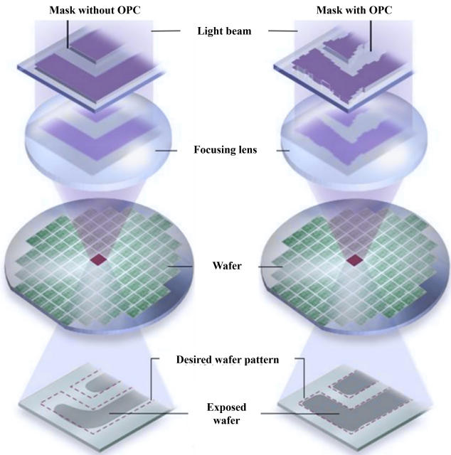
Pattern Distortion: Due to the uneven distribution of light intensity at the corners of patterns, rounding or chamfering occurs, leading to reduced corner accuracy. The light intensity at the ends of lines is weak, resulting in insufficient exposure of the photoresist. As a result, the length of the formed line ends is shorter than the designed length, a phenomenon known as line end shortening.
Spacing Deviation: The smaller the spacing between adjacent patterns, the more significant the mutual influence, and the greater the deviation between the actual spacing and the designed spacing. In severe cases, it may even lead to the adhesion of adjacent patterns.
As semiconductor manufacturing processes advance to nodes below 3 nm and 2 nm, the impact of the Optical Proximity Effect (OPE) becomes increasingly significant. Line width variation and pattern distortion can cause the Critical Dimension (CD) of devices to exceed the allowable error range, affecting the electrical performance of transistors such as switching speed and leakage current. To compensate for the proximity effect, it is necessary to narrow the adjustable range of process parameters such as exposure dose and focal length, leading to decreased process stability and reduced yield. In the era of Deep Ultraviolet Lithography (DUV) before Extreme Ultraviolet Lithography (EUV), the optical proximity effect was one of the core bottlenecks restricting the breakthrough of manufacturing processes to smaller nodes. To counteract the impact of the optical proximity effect, the industry has developed a series of mature correction technologies to compensate from multiple dimensions such as mask design and lithography process optimization:
· Optical Proximity Correction (OPC)
OPC is currently the most widely used correction technology. It counteracts pattern deviations during lithography by pre-distorting the mask patterns. Based on the optical model of the lithography process, it calculates the deviations of the actual lithographed patterns, and then reversely modifies the designed mask patterns. For example, adding “hammerhead” structures at the ends of lines, and adding “chamfer” or “rounded corner” compensations at the corners. It can be divided into two types: Rule-Based OPC and Model-Based OPC. The latter calculates the correction amount through precise optical and photoresist models, offering higher correction accuracy and being suitable for advanced manufacturing processes.

· Resolution Enhancement Technologies (RET)
RET is a general term for a series of technologies that improve lithography resolution and pattern fidelity. In addition to OPC, it includes Phase-Shifting Mask (PSM) and Off-Axis Illumination (OAI). The former introduces phase structures on the mask. By changing the phase of light, it causes destructive interference of diffracted light from adjacent patterns, enhances the light intensity contrast at pattern edges, and reduces proximity effects. The latter refers to changing the angle of incident light. By adjusting illumination modes (such as annular illumination and quadrupole illumination), it suppresses the interference of diffracted light and improves the resolution and contrast of patterns.
· Photoresist and Process Optimization
Develop photoresist materials with high contrast and high resolution to enhance the response sensitivity of photoresist to changes in light intensity, thereby reducing pattern deviations caused by uneven light intensity distribution. Optimize process parameters such as exposure dose, focal length, and baking temperature. Through fine adjustment of the process window, the impact of proximity effects is reduced.
At the 3 nm and below process nodes, especially after the adoption of Extreme Ultraviolet Lithography (EUV) technology, optical proximity effects present new characteristics and challenges. The EUV wavelength is only 13.5 nm, and diffraction effects are theoretically significantly weakened. However, due to the higher complexity of the EUV lithography optical system, lower photoresist sensitivity, and further reduction in pattern size, proximity effects remain a key issue to be addressed. Meanwhile, the higher cost of EUV masks places higher requirements on the accuracy and efficiency of OPC correction.
With the development of AI technology, machine learning and deep learning have been introduced into OPC correction and lithography model establishment. By training models with a large amount of process data, the accuracy and speed of correction are improved to meet the complex pattern correction requirements in advanced manufacturing processes. In addition, integrating lithography process constraints into the chip design stage in advance. Through Design-Manufacturing Co-Optimization (DFM), the impact of optical proximity effects is considered during chip placement and routing, thereby reducing correction difficulty from the source.

Contact us to learn more about our advanced electronic chemicals and speciality polymer materials, and how they can enhance your production performances.